What a Chip Actually Looks Like
Following an AI chip from design file to data center — with real photos
The Design
ARMThis is a stylized view of what ARM creates — a layout file (GDS-II format) that specifies every transistor, wire, and connection. CPU cores, cache, memory controllers, I/O — all defined at the nanometer level. This file is what gets sent to TSMC. ARM never touches physical material.
What ARM actually delivers
A set of GDS files. Imagine the world's most detailed architectural blueprint — except instead of rooms and walls, it describes billions of transistor positions across ~80 metal layers. The file for a modern chip can be hundreds of gigabytes.
- This is ARM's entire product. A file. That's it.
- Previously ARM just sold the CPU core design and other companies built full chips around it
- With the AGI CPU, ARM designed the entire chip for the first time
The Fabrication
TSMC
About the size of a dinner plate (12 inches). Each of those repeated squares is one chip die. A single wafer can yield dozens of large AI chip dies.
Each small square is a complete copy of ARM's chip. After printing, the wafer gets sliced ("diced") into individual dies — each one about 20-25mm per side.
What TSMC does physically
- Takes a blank silicon wafer — a perfectly flat, ultra-pure disc of silicon
- Prints ARM's design onto it — 80+ layers, using EUV lithography (13.5nm wavelength light)
- Each layer: deposit material → coat with light-sensitive resist → blast with EUV light through a mask → etch away exposed areas → repeat
- Takes ~3 months from blank wafer to finished wafer with all layers printed
- Then dices the wafer into individual dies with a diamond-tipped saw
- TSMC also fabs the silicon interposer — the "highway" that will connect the CPU die to memory later
Advanced Packaging (CoWoS)
TSMC or OSAT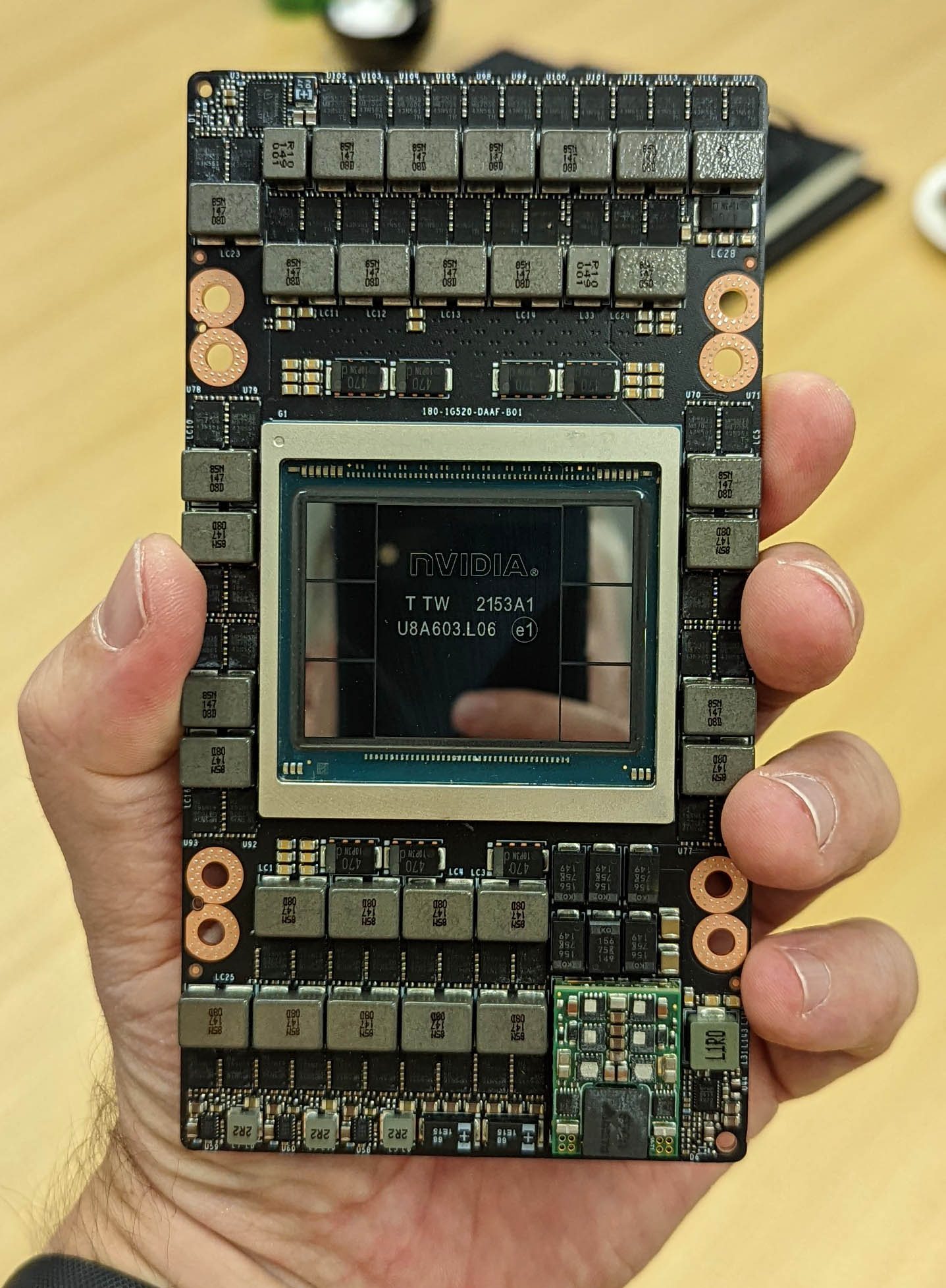
The large shiny rectangle in the center is the GPU die (Nvidia-designed, TSMC-fabricated). The 6 smaller rectangles around it are HBM3 memory stacks (SK Hynix). All of these sit on a silicon interposer that you can't see — it's underneath, connecting everything. The green PCB around it is the SXM module board.
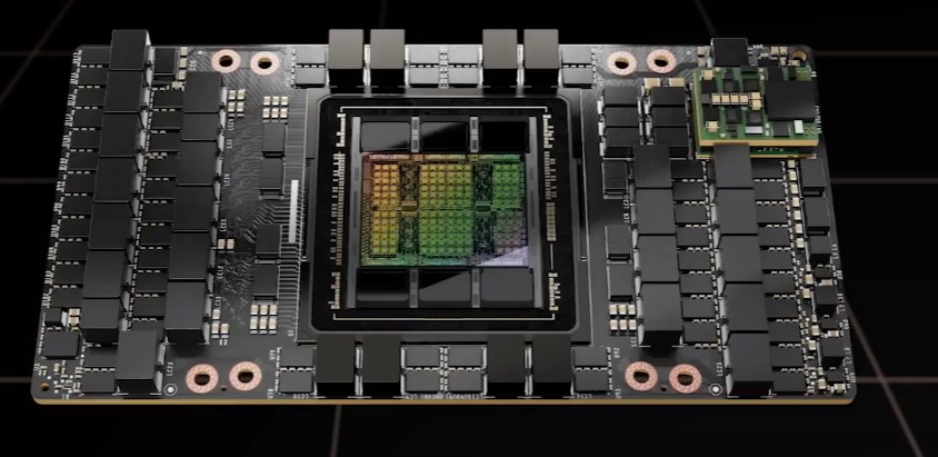
This shows the module more clearly. The package (center silver area) contains the GPU die + HBM stacks on the interposer. Everything around it — capacitors, power regulation, connectors — makes up the module that slots into a server.
What happens during advanced packaging
This is where loose silicon dies become a working chip. Think of it as building a tiny city:
- Step 1: Take the silicon interposer (TSMC-fabricated thin wafer with through-silicon vias)
- Step 2: Place the CPU die and HBM memory stacks face-down onto the interposer using micro-bumps (~25μm solder balls — thinner than a human hair)
- Step 3: This interposer "sandwich" gets flipped and mounted onto an organic package substrate using larger C4 bumps
- Step 4: Fill gaps with underfill epoxy for structural strength
- Step 5: Attach heat spreader lid on top with thermal paste
- Step 6: Attach BGA solder balls on the bottom (what plugs into the server board)
TSMC can print silicon faster than it can package it. CoWoS capacity — not fab capacity — is what's constraining the AI chip supply chain. This is exactly why TSMC is licensing packaging tech to ASE and Amkor. The demand for advanced packaging is growing faster than anyone can build clean rooms to do it.
Assembly, Test & Ship
ASE / AMKORFlip the chip over and this is what you see — a grid of tiny solder balls (Ball Grid Array). Each ball is a connection point. An H100 has ~5,000+ BGA balls. The OSAT attaches every one.
Automated test equipment runs every chip through exhaustive testing — power-on, logic verification, burn-in at high temperature, speed characterization. Chips that pass get "binned" by performance tier. The fastest chips command premium prices.
What the OSAT does (the less glamorous but critical work)
- Receives: Bare CPU dies from TSMC, HBM stacks from SK Hynix, interposers from TSMC, substrates from Ibiden/Shinko
- Assembles: Mounts everything together through a sequence of soldering, bonding, underfilling, and lid attachment steps
- Tests: Every finished chip gets run through burn-in testing (high temp/voltage for hours), functional testing, and speed binning
- Ships: Finished, tested chips in anti-static trays to Meta, OpenAI, Cloudflare, etc.
- Yield matters: If the OSAT's process damages chips during assembly, that's revenue destroyed. The precision is extreme — micro-bumps are 25μm (a human hair is 70μm)
In the Data Center
The finished chip ends up here
The packaged chip gets soldered onto a module board (like the H100 SXM board in the photo above), which slots into a server tray (like NVIDIA's DGX systems), which goes into a rack in a data center owned by Meta, OpenAI, or whoever bought it. From ARM's design file to a running AI workload in a data center: ~6-9 months total.
Every AI chip that ships passes through this chain. ARM captures value at the top (design IP). TSMC captures the most (fab + interposer + some packaging). ASE and Amkor capture value at the bottom (assembly + test). SK Hynix captures memory. Teradyne/Advantest capture test equipment.
The constraint right now isn't design or even fab — it's packaging. Which is why ASE's advanced packaging revenue is more than doubling year-over-year, and Amkor is building a $7B campus in Arizona.